
Printed circuit board assembly is abbreviated as PCBA. PCBA is the most important step in electronics manufacturing. Our site pcba.app reveals everything about PCB assembly and related things.
PCBA is a printed circuit board mounted with components and plays the main functions of the expected products. PCB assembly or PCBA manufacturing is usually completed by a third-party contract electronics manufacturer.
You can understand what a PCBA is by understanding a few questions: 1. what is a PCB and what is a PCBA? 2. What do the PCBA-related abbreviated terms mean? 3. What is the price of PCBA?
1. what is a PCB and what is a PCBA?
A PCBA is an assembled PCB, and a PCB is a bare printed circuit board laminated in insulation layers and conductive layers.
Printed Circuit Board
Printed circuit boards have various substrate material options, such as FR4 (epoxy fiberglass), polyimide (abbreviated for PI, rigid-flex and flexible PCBs use this substrate material), ceramic (including aluminum nitride and aluminum oxide), polytetrafluoroethylene (abbreviated for PTFE, high-frequency PCBs use this substrate material), metal (including aluminum and copper).
A PCB mainly consists of a substrate, prepreg (abbreviated for PP, which is an insulation and bonding layer between copper layers and the substrate), and copper wires (conductive layers interconnected by plating through holes or other PCB vias). On the component-mounting side, there are copper pads or joints for soldering, which are applied with surface finishes. There are through holes for soldering and positioning holes on the board. Besides, the PCB is sprayed with solder mask to insulate the board and silkscreen for component marks and board information display.
PCBA
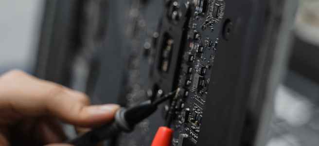
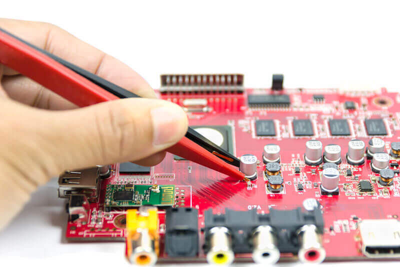
A PCBA is an assembled PCB mounted with electronic components without the enclosure assembled. The PCB pads and surface-mount components (SMD) are soldered by surface-mount technology (SMT), and the through-holes and PTH components are soldered by through-hole technology (THT or DIP).
A PCBA may require only SMT or THT or both SMT and THT. If your PCB requires both assembly techniques, SMT assembly happens before THT assembly.
SMT assembly is automatic, while THT assembly is half-automatic.
The SMT assembly process includes silkscreen printing solder paste on PCB pads, SPI, picking and placing SMDs on PCB pads, x-ray inspection, reflow soldering, and AOI inspection.
The THT assembly process includes fitting PTH components’ pins through the through-holes and wave soldering or selective soldering.
2. What do the PCBA-related abbreviated terms mean?
If you are new to having PCBA manufactured, PCBA-related abbreviations without full words and explanations are annoying. You can make clear these PCBA-related abbreviations now.
(I’m sure you don’t need more explanations for PCB, PCBA, SMT, SMD, and THT from the above content, so I just go ahead for others.)
PWB: printed wiring board, it is another name for PCB used in some countries such as Japan.
PCA: printed circuit assembly, it is another name for PCBA used in some countries such as France.
AOI: automatic optical inspection, which makes sure there’s no open/short circuit and soldering bridge. During PCB assembly, it is a necessary inspection before or after reflow soldering in the SMT process. In PCB fabrication, it applies after each circuit layer is etched out.
BGA: ball grid array, which is an IC package method. The BGA parts replace pins with solder balls. During PCB assembly, if there are BGAs, the PCBA must undergo an x-ray inspection before reflow soldering to make sure the solder balls of the BGA are good for soldering.
IC: integrated circuits, which integrate hundreds and thousands of electronic components on a tiny semiconductor. The smallest space between electronic components on an IC is 3 nanometers currently.
SPI: solder paste inspection, an inspection after silkscreen printing solder paste on PCB pads. It scans the solder paste on PCB pads and makes sure the solder paste thickness, size, and position are qualified for soldering.
FAI: first article inspection, which means PCBA sample testing. Before bulky PCBA production, we have to first manufacture 5 pieces and pick up one by chance. We inspect every electronic component value on the PCBA to make sure it is qualified. Then we generate an FAI report for our customers to review and approved bulky production.
BOM: bill of materials, which is an excel that lists the information of electronic components used for PCB assembly. By sending a BOM to the PCBA manufacturer, the manufacturer can source all electronic components for you and review your project before putting it into production.
DFM: design for manufacturing. A PCB manufacturer can do it for you to make sure your PCB design can be put into fabrication.
DFA: design for assembly. A PCBA manufacturer can do it for you to make sure your PCBA can be a success before assembly.
DFX: design for excellence. A box build manufacturer can do it for you to make sure your end product is a success before assembling the enclosure to the PCBA.
Besides, you may want to know Gerber. Gerber is not an abbreviation. It is a PCB design graphic file containing each layer’s specifications.
3. What is the price of PCBA?
PCBA is a custom product so its price is not fixed. To know how much your PCBA will cost, you need to send your BOM and Gerber to an electronics contract manufacturer to get a quotation.
The PCBA price usually contains the PCB fabrication price, PCB testing price, DFM, PCB assembly price, DFA, electronic components price, functional jig price, and DFX. If you need value-added services, such as conformal coating, IC programming, burn-in testing, and box-build assembly, their prices also add to the PCBA price.
Conclusion
PCBA is the semi-product of everything. If you want to have PCBA designed and manufactured, don’t miss the one-stop PCBA source factory .
